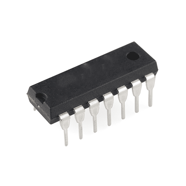
74164 (8-bit serial-in/parallel-out shift register)
SKU: 22687
Pick up from store
Shipping 2-3 business days
Description
The 74164 is an 8-bit serial-in/parallel-out shift register. It is part of the 7400 series of ICs and is commonly used in digital systems for applications where you need to convert serial data to parallel data or vice versa. The IC can take in serial data (bit by bit) and output it in parallel (all bits simultaneously). It’s widely used for data storage, data transfer, and shift register applications.
74164 IC Description:
The 74164 is an 8-bit serial-in/parallel-out shift register with a clocked operation. It is designed to accept serial data at its serial input (DS) pin and shift the data into the register on the rising edge of the clock (CLK) signal. Once the data is shifted in, it can be output in parallel form from Q0 to Q7. The 74164 also includes a serial output (QH) for serial data retrieval.
Key Features:
- 8-bit Serial-in, Parallel-out Shift Register: The 74164 has 8-bit data storage, and it can shift in data serially while outputting the stored data in parallel.
- Clocked Operation: The shift register operates in synchronous mode, with data shifting occurring on the rising edge of the clock signal.
- Parallel Outputs (Q0 to Q7): The IC provides 8 parallel outputs, one for each bit of data stored in the shift register.
- Serial Output (QH): The serial output allows for the shifted data to be accessed one bit at a time.
- Shift Control: The data is shifted with each clock pulse, either to the left or right depending on the configuration of the circuit.
Pin Configuration (16-pin package):
Here’s the pinout for the 74164:
- Pin 1 (Q0): Output bit 0 (Least Significant Bit).
- Pin 2 (Q1): Output bit 1.
- Pin 3 (Q2): Output bit 2.
- Pin 4 (Q3): Output bit 3.
- Pin 5 (Q4): Output bit 4.
- Pin 6 (Q5): Output bit 5.
- Pin 7 (Q6): Output bit 6.
- Pin 8 (Q7): Output bit 7 (Most Significant Bit).
- Pin 9 (Serial Output): QH - Serial data output.
- Pin 10 (Shift/Load): Shift/Load input, controls whether data is shifted or loaded in parallel.
- Pin 11 (Clock): CLK - Clock input for synchronizing the shifting of data.
- Pin 12 (Serial Data Input): DS - Serial data input for shifting data into the register.
- Pin 13 (Ground): Ground.
- Pin 14 (Vcc): Supply voltage (typically 5V).
- Pin 15 (Clear): Active-low Clear input for resetting the shift register.
- Pin 16 (Output Enable): OE - Output enable for controlling parallel outputs.
Related Products
MAX485 TTL To RS485 Converter Module
74259 (8-bit addressable latch )
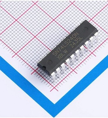
74240 (Octal 3-STATE Buffer/Line Driver/Line Receiver IC DIP-20 )
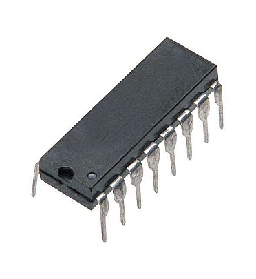
74160 (Synchronous 4-Bit Counter)
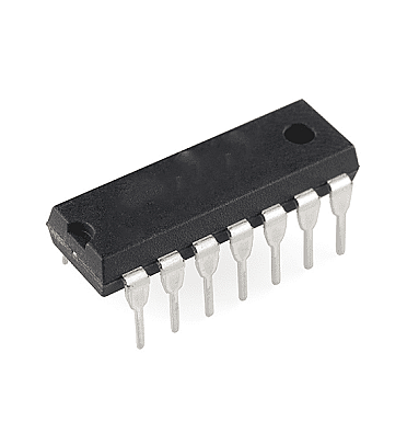
7437 (2-input NAND Gates)
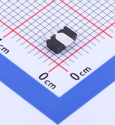
AMS1117 - ADJ - SOT-89 (ADJ Linear Voltage Regulator)
AMS1117 - 5 - SOT-89 (5V Linear Voltage Regulator)