
No products in the cart.

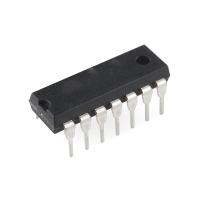
7495 ( 4-bit Binary shift register )
In Stock
EGP23.00
In Stock
Add to WishlistRemove from Wishlist
CompareAdd to Wishlist
Description
The 7495 is a 4-bit binary shift register with parallel load and serial input. It is part of the 7400 series of integrated circuits and is used for storing and shifting binary data. The IC can shift data in either direction (left or right) and supports parallel loading of data for immediate access.
7495 IC Description:
The 7495 is a 4-bit shift register that allows for both serial and parallel data transfer. It can store 4 bits of data and shift this data in serial form either left or right. It also supports parallel loading, meaning you can load 4 bits of data into the register at once. This IC is useful in applications like serial-to-parallel or parallel-to-serial conversion, and can be used for data storage and manipulation in digital systems.
Key Features:
- 4-bit Shift Register: It can store and shift 4 bits of binary data.
- Shift Left or Right: The shift direction can be controlled via the Shift/Load pin.
- Parallel Load: The IC supports parallel loading of 4 bits of data, allowing you to load a full 4-bit word into the shift register simultaneously.
- Serial Input: The IC has a serial data input pin for shifting data in one bit at a time.
- Clocked Operation: The shift register is clocked, meaning it shifts data on the rising edge of the clock signal.
- Clear Pin: The IC includes an active-low clear pin to reset the register to all zeros.
- TTL Compatible: The 7495 IC is TTL-compatible, which makes it easy to interface with other TTL logic devices.
Pin Configuration (16-pin package):
Here is the pinout for the 7495 4-bit shift register:
- Pin 1 (Q0): Output bit 0 (least significant bit).
- Pin 2 (Q1): Output bit 1.
- Pin 3 (Q2): Output bit 2.
- Pin 4 (Q3): Output bit 3 (most significant bit).
- Pin 5 (Clear): Active-low clear input. Clears all outputs to 0 when LOW.
- Pin 6 (Shift/Load): This pin controls the operation of the shift register:
- LOW: Shift register mode (shifts data on the clock pulse).
- HIGH: Parallel load mode (loads data from D0-D3).
- Pin 7 (Clock): The clock input. Data shifts or loads on the rising edge of the clock.
- Pin 8 (D0): Data input bit 0 for parallel loading.
- Pin 9 (D1): Data input bit 1 for parallel loading.
- Pin 10 (D2): Data input bit 2 for parallel loading.
- Pin 11 (D3): Data input bit 3 for parallel loading.
- Pin 12 (Serial Input): Serial data input for shifting.
- Pin 13 (Shift Out): Serial data output after shifting.
- Pin 14 (Vcc): Supply voltage (typically 5V).
- Pin 15 (Ground): Ground connection.
- Pin 16 (Serial Output): Serial output from the shift register.
How It Works:
- Shift Register Mode (Shift Left or Right):
- When the Shift/Load pin is LOW, the IC operates in shift register mode. In this mode, data is shifted through the register bit by bit with each rising edge of the clock. The direction of the shift (left or right) is determined by the serial input and serial output pins.
- Data is shifted from the serial input (pin 12) into the register, and the shifted bits are available at the Q0 to Q3 outputs (pins 1 to 4). If the shift is left, the bit enters from the leftmost side, and if the shift is right, the bit enters from the rightmost side.
- Parallel Load Mode:
- When the Shift/Load pin is HIGH, the shift register operates in parallel load mode. In this mode, the 4-bit data present on the D0 to D3 inputs (pins 8 to 11) is loaded into the shift register directly. This allows you to load a 4-bit value into the register in one operation.
- Clear Operation:
- The Clear pin (pin 5) is active-low, meaning that when this pin is LOW, it will reset all the outputs (Q0 to Q3) to 0.
- Clocking:
- The Clock pin (pin 7) is used to trigger the shifting or loading process. On the rising edge of the clock pulse:
- In shift mode, data is shifted left or right.
- In load mode, the data on the D0 to D3 inputs is loaded into the register.
- The Clock pin (pin 7) is used to trigger the shifting or loading process. On the rising edge of the clock pulse:
Truth Table:
| Shift/Load (S/L) | Clear (CLR) | Clock (CLK) | Data (D0-D3) | Operation | Outputs (Q0-Q3) |
|---|---|---|---|---|---|
| 0 (Shift) | 1 (Inactive) | Rising Edge | – | Shift data left or right | Shifted Data |
| 1 (Load) | 1 (Inactive) | Rising Edge | D0-D3 | Load data from D0-D3 into register | Loaded Data |
| – | 0 (Clear) | – | – | Clear register (reset to 0) | 0000 |
Applications:
- Data Shift/Storage: The 7495 can be used in applications where data needs to be stored and then shifted serially or parallelly. It is useful for data conversion between serial and parallel formats.
- Serial-to-Parallel and Parallel-to-Serial Conversion: The IC can convert serial data into parallel data (by shifting it in) or convert parallel data into serial data (by shifting it out).
- Data Transfer in Digital Circuits: It is used for transferring data between different parts of a system, especially when the system requires parallel loading of data or serial shifting of data.
- Timing and Sequencing: The IC can be used in timing or sequencing applications where the state of each output (Q0 to Q3) represents different steps or events in a process.
- Counters and Registers: It can serve as a counter or register in digital logic circuits. For example, it could be used in binary counters where data is shifted at regular clock intervals.
- LED Drivers: It can be used to drive LEDs or other indicator devices in a serial-to-parallel fashion. For example, the IC can shift data serially into the register, and then the parallel outputs can drive LEDs directly.
Electrical Characteristics:
- Supply Voltage (Vcc): Typically 5V (with a range of 4.5V to 5.5V).
- Current Consumption: As a CMOS device, the 7495 IC operates with low power consumption.
- Output Drive Capability: The IC is capable of driving standard TTL-level logic circuits and LEDs directly.
Example Circuit:
In a simple serial-to-parallel conversion application, the 7495 IC can be used to shift in serial data bit by bit through the serial input (pin 12). Once the desired number of bits have been shifted in, the parallel outputs (Q0 to Q3) will contain the 4-bit data, which can be used to drive LEDs, display values, or perform further processing in the circuit.
Only logged in customers who have purchased this product may leave a review.
Related products


- Image
- SKU
- Rating
- Price
- Stock
- Availability
- Add to cart
- Description
- Content
- Weight
- Dimensions
- Additional information
Reviews
There are no reviews yet.