
No products in the cart.
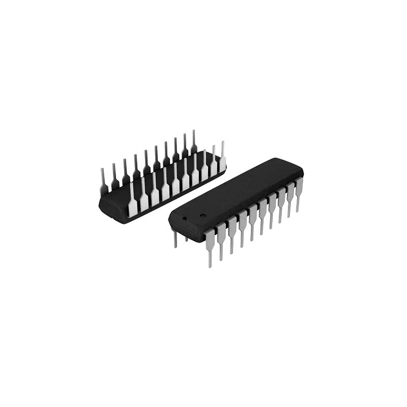
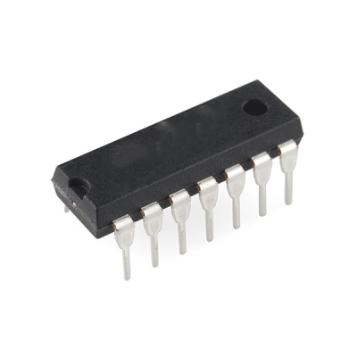
74LS240 (Octal 3-state buffer)
In Stock
EGP25.00
In Stock
Add to WishlistRemove from Wishlist
CompareAdd to Wishlist
Description
The 74×240 (ex 74HC240) is a chip that contains eight inverting buffer/drivers with tri-state outputs. This configuration is particularly useful for driving data buses and providing temporary output isolation.
In this guide, you’ll learn the things you need to know about this chip in order to effectively use buffer/drivers in your own projects.
What does the 74HC240 / 74LS240 do?
The 74×240 is an octal buffer/line driver, meaning it has eight (octal) buffer gates. It is used to send signals from one part of a circuit to another without weakening them.
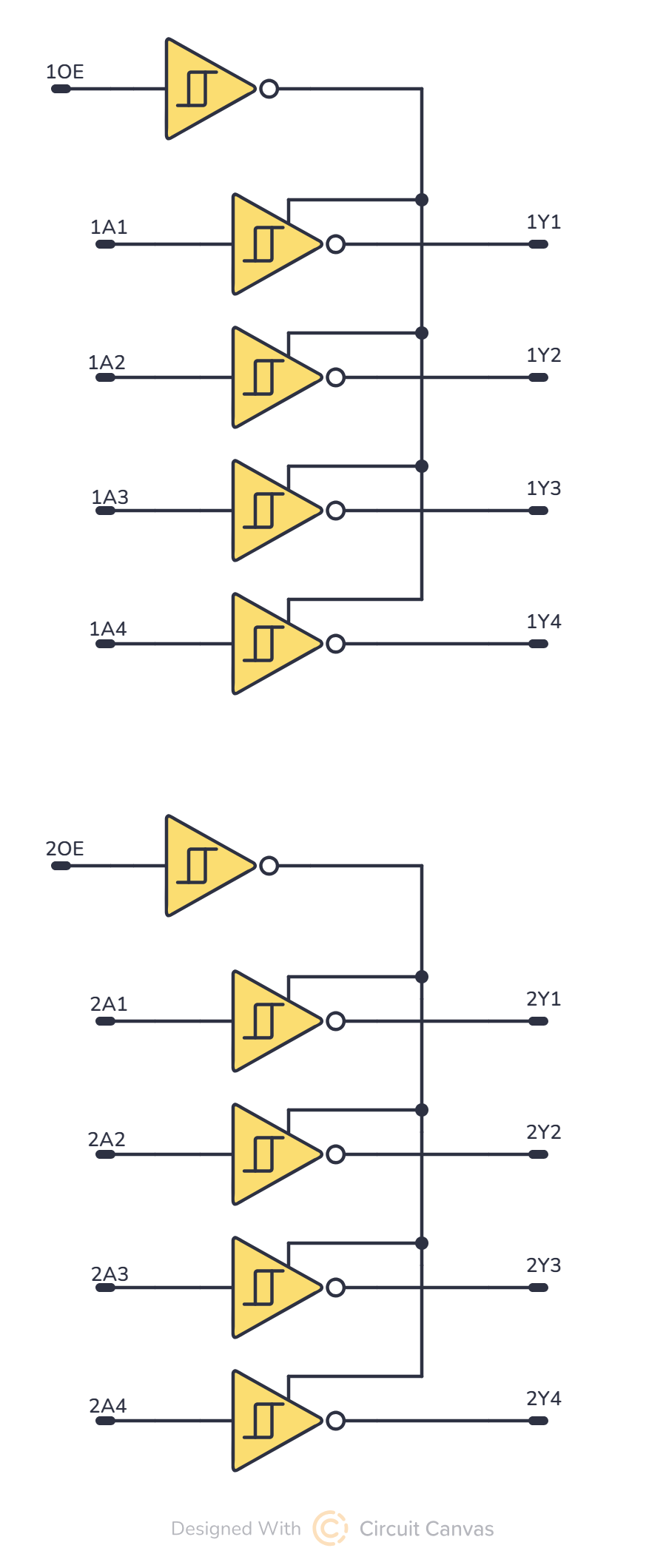
This chip has three-state outputs, so it can drive high (send a strong signal), drive low (send no signal), or be in a high-impedance state (like it’s disconnected). The high-impedance state lets multiple devices share the same output lines without interfering with each other.
The 74×240 has two sets of four buffer gates, and each set is controlled by an enable pin. When the enable pin is low, the buffers are active. The chip also inverts, or flips, the input signal. This means a high input becomes low, and a low input becomes high.
This makes the 74×240 convenient for controlling data flow in circuits. It is often used in computers, communication devices, and more!
How To Use This Chip
The 74HC240 comes in a 20-pin package. Most 7400 ICs support a VCC voltage of 5V. But one difference between the HC and LS version of the chip is that the 74HC240 supports 2V to 6V, while the 74LS240 only supports 5V.
The 74HC240 can supply up to 6 mA of current from an output pin. The 74LS240 can sink 24 mA and source 15 mA of current from an output pin.
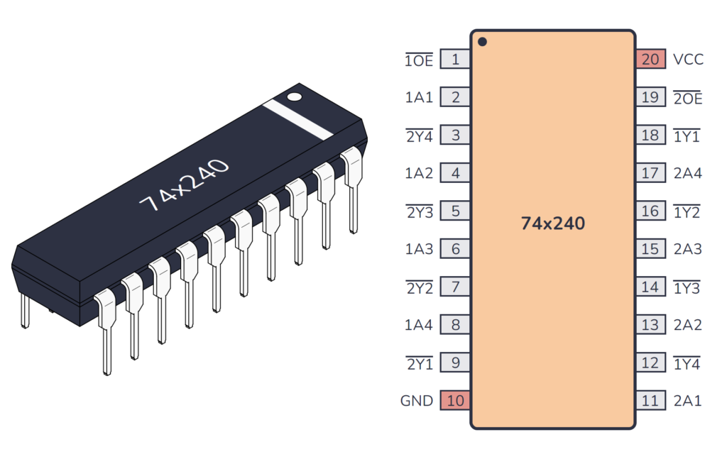
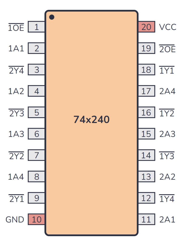
74×240 Pinout
The 74×240 has 20 pins and contains two 4-bit 3-state inverting buffer/line driver laid out as shown in the pinout diagram below:
| Pin Name | Pin # | Type | Description |
|---|---|---|---|
| 1OE | 1 | Input | Output Enable for the first set of four buffers (active low). |
| 1A1 | 2 | Input | First input to the first set of four buffers. |
| 1Y1 | 3 | Output | Inverted output from the first buffer. |
| 1A2 | 4 | Input | Second input to the first set of four buffers. |
| 1Y2 | 5 | Output | Inverted output from the second buffer. |
| 1A3 | 6 | Input | Third input to the first set of four buffers. |
| 1Y3 | 7 | Output | Inverted output from the third buffer. |
| 1A4 | 8 | Input | Fourth input to the first set of four buffers. |
| 1Y4 | 9 | Output | Inverted output from the fourth buffer. |
| GND | 10 | Power | Connect to ground (GND). |
| 2A1 | 11 | Input | First input to the second set of four buffers. |
| 2Y1 | 12 | Output | Inverted output from the fifth buffer. |
| 2A2 | 13 | Input | Second input to the second set of four buffers. |
| 2Y2 | 14 | Output | Inverted output from the sixth buffer. |
| 2A3 | 15 | Input | Third input to the second set of four buffers. |
| 2Y3 | 16 | Output | Inverted output from the seventh buffer. |
| 2A4 | 17 | Input | Fourth input to the second set of four buffers. |
| 2Y4 | 18 | Output | Inverted output from the eighth buffer. |
| 2OE | 19 | Input | Output Enable for the second set of four buffers (active low). |
| VCC | 20 | Power | Positive power supply. Connect to +5V power. |
Datasheet for the 74LS240
Download the PDF datasheet for your version of the 74×240 here:
Only logged in customers who have purchased this product may leave a review.


- Image
- SKU
- Rating
- Price
- Stock
- Availability
- Add to cart
- Description
- Content
- Weight
- Dimensions
- Additional information
Reviews
There are no reviews yet.