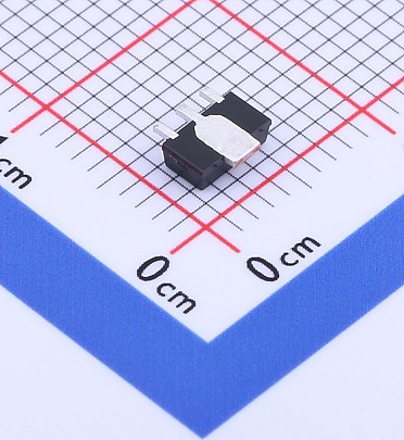
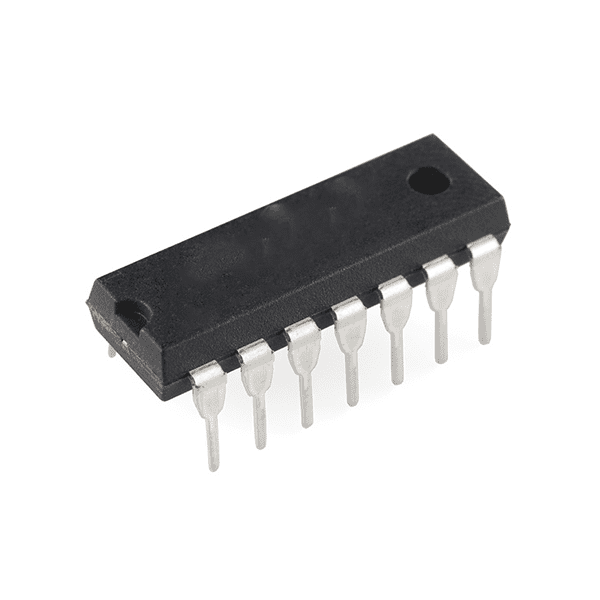
74195 (8-bit Shift Register)
SKU: 22690
Pick up from store
Shipping 2-3 business days
Description
The 74195 is an 8-bit Shift Register with parallel load and serial in/out functionality. It is part of the 7400 series of ICs and is typically used in digital systems to store and shift data. The 74195 IC is widely used in applications requiring the serial-to-parallel or parallel-to-serial conversion of data.
74195 IC Description:
The 74195 is an 8-bit Shift Register that can be used to store data and shift it in or out either serially or in parallel. It is commonly used in digital systems for data storage, serial-to-parallel conversion, and parallel-to-serial conversion. The shift register has parallel load functionality, allowing it to capture and hold data from the parallel inputs when a load signal is given.
Key Features:
- 8-bit Shift Register: The 74195 has 8 bits of storage, meaning it can store and shift 8 bits of data.
- Serial Data Input (DS): It has a serial input (DS) for shifting data in one bit at a time.
- Parallel Data Input (D0–D7): It also has parallel data inputs for loading the shift register with 8 bits of data in parallel.
- Shift Control: The IC allows data to be shifted left or right, controlled by the Shift/Load (S/L) pin.
- Serial Output (QH): The 74195 has a serial output (QH) that outputs the shifted data.
- Clocked Operation: The register is clocked, meaning data is shifted or loaded on the rising edge of the clock signal.
- Active-Low Reset (MR): The IC includes an active-low reset input, which clears the data in the register when low.
- Enable Pin: The Output Enable (OE) pin controls whether the data is output from the register.
Pin Configuration (16-pin package):
Here’s the pinout for the 74195:
- Pin 1 (QH): Serial output of the shift register.
- Pin 2 (Q0): Parallel output bit 0.
- Pin 3 (Q1): Parallel output bit 1.
- Pin 4 (Q2): Parallel output bit 2.
- Pin 5 (Q3): Parallel output bit 3.
- Pin 6 (Q4): Parallel output bit 4.
- Pin 7 (Q5): Parallel output bit 5.
- Pin 8 (Q6): Parallel output bit 6.
- Pin 9 (Q7): Parallel output bit 7.
- Pin 10 (MR - Master Reset): Active-low reset input. Resets all data to 0.
- Pin 11 (Shift/Load): Shift/Load control input.
- Pin 12 (Clock): Clock input for shifting data.
- Pin 13 (Parallel Data Inputs D0 to D7): 8-bit parallel data input (D0 to D7).
- Pin 14 (Serial Data Input): Serial input for shifting data in (DS).
- Pin 15 (Vcc): Supply voltage (typically 5V).
- Pin 16 (Output Enable - OE): Active-low output enable input.
Related Products

OLFA Plastic Cutter Knife for Hook Blades (Acrylic Cutting)
MAX485 TTL To RS485 Converter Module
74259 (8-bit addressable latch )
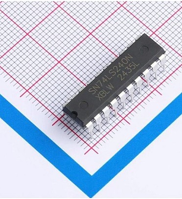
74240 (Octal 3-STATE Buffer/Line Driver/Line Receiver IC DIP-20 )
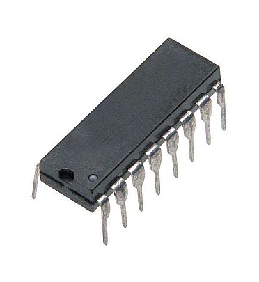
74160 (Synchronous 4-Bit Counter)
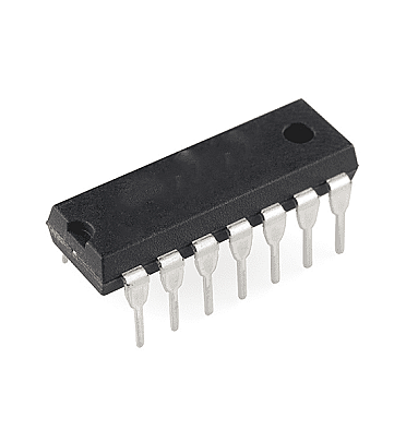
7437 (2-input NAND Gates)
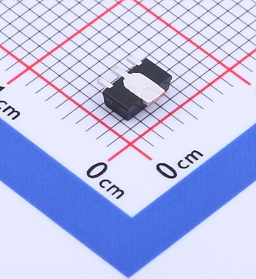
AMS1117 - ADJ - SOT-89 (ADJ Linear Voltage Regulator)