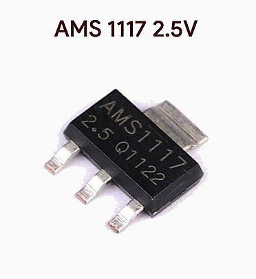
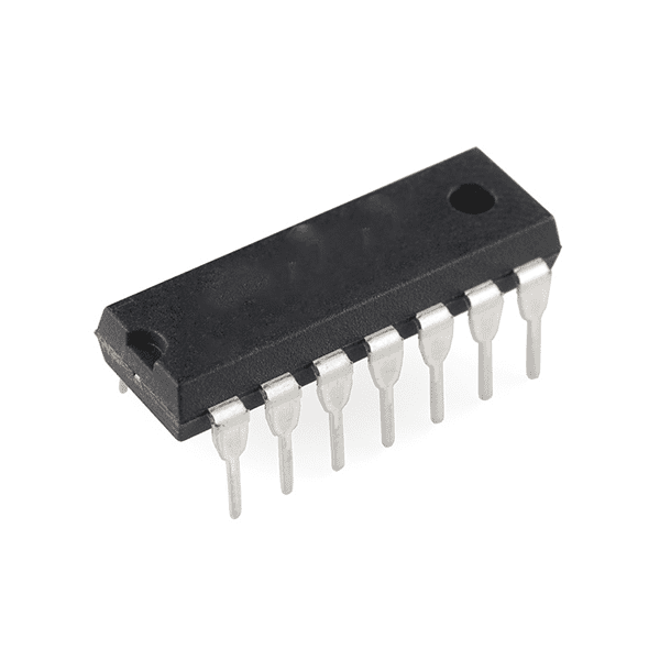
CD4015 (Dual 4-bit Static Shift Register)
SKU: 14144
Pick up from store
Shipping 2-3 business days
Description
CD4015 - Dual 4-bit Static Shift Register
The CD4015 is a dual 4-bit static shift register IC, meaning it can shift data in or out serially or store data in parallel. This chip is part of the CD4000 series of CMOS logic ICs, which are designed for low power consumption and high noise immunity.
It is a commonly used device in digital circuits where data needs to be shifted or stored, and it can function both in serial-to-parallel and parallel-to-serial modes. The CD4015 is typically used in applications such as data storage, data transfer, serial communication, LED displays, and timing circuits.
Key Features:
- Dual 4-bit Register:The IC contains two independent 4-bit shift registers, which allows for dual-channel operation. Each register can hold 4 bits of data, providing a total of 8 bits of data storage.
- Shift Register Mode:The CD4015 can shift data serially (bit by bit) either into or out of the register. This makes it useful for transferring data across fewer pins or for serial communication purposes.
- Parallel Loading:The shift register supports parallel loading, meaning you can load the shift register with 4 bits of data at once through parallel inputs.
- Shift Right and Shift Left:Data can be shifted in both directions (right and left) using dedicated control pins, providing flexibility for various data manipulation applications.
- Clear Function:The clear (reset) pin allows you to reset the register, clearing the stored data (all bits set to zero), ensuring a predictable state before shifting or storing new data.
- Low Power Consumption:Like most CMOS devices, the CD4015 is designed to consume minimal power, making it suitable for battery-powered or low-energy circuits.
- Flexible Logic Levels:The CD4015 works with logic levels compatible with the CMOS family, allowing for compatibility with other CMOS devices.
- High Noise Immunity:CMOS technology provides the IC with high noise immunity, making it reliable for operation in noisy environments.
Pinout Configuration (16-Pin DIP Package):
- Pins 1-4 (Shift Register 1 - Parallel Data Inputs):
- These pins are for the parallel loading of data into the first shift register.
- Pin 5 (Shift Left/Right Control - Register 1):
- This pin determines the shift direction for the first register.
- Pin 6 (Shift Clock - Register 1):
- This pin is used to clock the data into or out of the first register.
- Pin 7 (Output - Register 1):
- This pin outputs the data stored in the first shift register.
- Pin 8 (Clear/Reset):
- When activated, this pin resets the contents of both shift registers to zero.
- Pins 9-12 (Shift Register 2 - Parallel Data Inputs):
- These pins are for the parallel loading of data into the second shift register.
- Pin 13 (Shift Left/Right Control - Register 2):
- This pin determines the shift direction for the second register.
- Pin 14 (Shift Clock - Register 2):
- This pin is used to clock the data into or out of the second register.
- Pin 15 (Output - Register 2):
- This pin outputs the data stored in the second shift register.
- Pin 16 (Vcc):
- Power supply pin (typically 5V for CMOS logic ICs).
Related Products
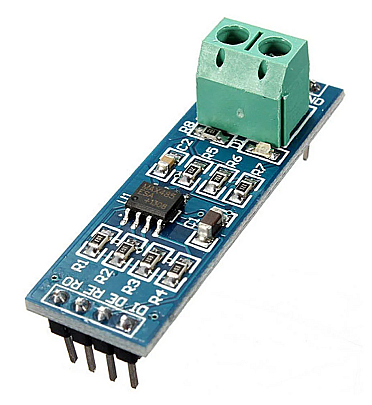
MAX485 TTL To RS485 Converter Module
AMS1117 - ADJ - SOT-89 (ADJ Linear Voltage Regulator)
AMS1117 - 5 - SOT-89 (5V Linear Voltage Regulator)
AMS1117 - 2.5 - SOT-89 (2.5V Linear Voltage Regulator)
AMS1117 - 1.8 - SOT-89 (1.8V Linear Voltage Regulator)
AMS1117 - 1.5 - SOT-89 (1.5V Linear Voltage Regulator)
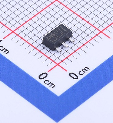
AMS1117 - 1.2 - SOT-89 (1.2V Linear Voltage Regulator)